AOI Optical Inspection
Automated optical inspection compares every board against its reference image after reflow, catching missing, misplaced, tombstoned and polarity-reversed components. Five AOI systems are installed across the lines.
Manufacturing Capabilities
Equipment, capacity and process windows available on our production floor in Nansha, Guangzhou — organised by bare board fabrication, PCB assembly, production equipment and inspection.
PCB Fabrication
Bare board specifications. Fabrication ends with an unpopulated, surface-finished board ready for solder paste printing.
| Parameter | Capability |
|---|---|
| PCB layer count | 2 – 32 layers |
| Minimum via diameter | 0.15 mm |
| HDI processing | Supported |
| Surface finishes | HASL / ENIG / OSP / hard gold |
| Prototype bare board supply | Quick-turn sampling available |
| Supply route | In-house fabrication capability and qualified manufacturing partners |
Bare boards are produced through our own fabrication capability and qualified manufacturing partners, so the process and lead time can be matched to each project.
PCBA Assembly
Assembly process window, from the smallest component we can place to the largest board we can run.
| Parameter | Capability |
|---|---|
| Minimum component size | 01005 (0.4 × 0.2 mm) |
| Minimum BGA ball pitch | 0.3 mm |
| Minimum QFN lead pitch | 0.4 mm |
| Maximum PCB assembly size | 350 × 250 mm |
| Solder type | Leaded / lead-free SAC305 |
| Reflow peak temperature | Up to 260 °C, profile customisable |
| Panelisation | V-cut / stamp holes / bridge |
The maximum board size of 350 × 250 mm applies to PCB assembly — the size of board that can be processed through our SMT and through-hole lines. It is not a bare board fabrication limit.
Production Equipment & Capacity
Six automated SMT production lines, supported by automatic printing, SPI, reflow and optical inspection equipment.
| Equipment | Installed |
|---|---|
| High-speed placement machines | 8 |
| Multi-function placement machines | 6 |
| Automatic solder paste printers | 6 |
| Ten-zone reflow ovens | 4 |
| AOI optical inspection systems | 5 |
| SPI solder paste inspection systems | 6 |
| Wave soldering / selective wave soldering | 1 |
| X-ray inspection system | 1 |
Inspection Capabilities
Inspection is distributed through the process — it is not a single gate at the end of the line.
Automated optical inspection compares every board against its reference image after reflow, catching missing, misplaced, tombstoned and polarity-reversed components. Five AOI systems are installed across the lines.
Solder paste volume, area and height are measured after printing at six SPI stations, so an under-printed or bridging stencil is corrected before a single component is placed.
X-ray inspection looks inside the joints that cannot be seen from the outside — BGA balls, QFN thermal pads and other hidden solder joints on high-density assemblies.
In-circuit testing verifies component presence, value and orientation, and checks for open and short circuits across the assembled board.
Functional testing powers the assembly up and exercises it against an agreed specification, so the board is proved to work and not merely to be built correctly.
Burn-in and ageing tests run assemblies under load for an agreed period to surface early-life failures before the product ever reaches the customer.
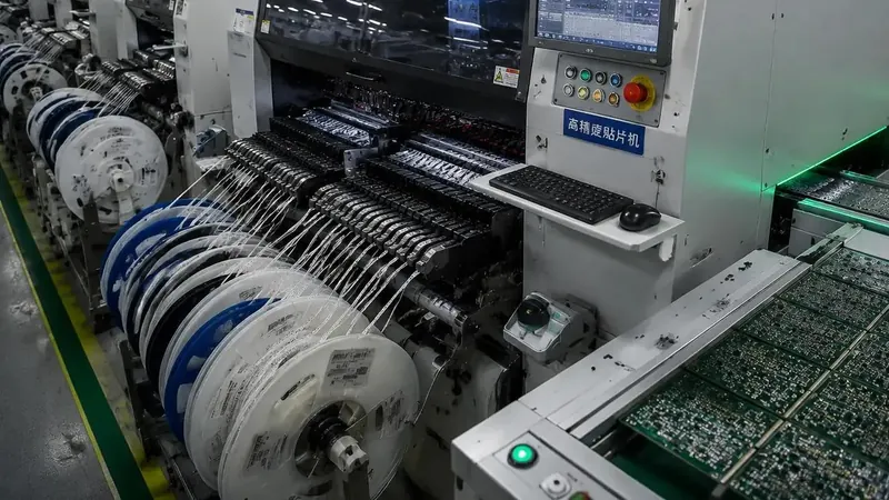
The figures on this page describe what our lines are configured to run today: multilayer boards from 2 to 32 layers, components down to 01005, fine-pitch BGA and QFN devices, and mixed SMT and through-hole assemblies up to 350 × 250 mm.
If your design sits outside any of these windows, tell us at enquiry stage. We will either confirm how we can process it or say plainly that it is not a good fit — before you commit to an order.
Request a QuoteRequest a Quote
Contact our team to discuss your PCB fabrication and PCBA assembly requirements. Send us your Gerber files and BOM and we will come back with a manufacturing quotation, usually within 24 hours.
Your enquiry goes directly to our sales team by e-mail.